JK FlipFlop
April 8, 2015
Here we have an NAND RS Flip-flop (+ updated to an JK FF) with an edge-triggered input.
A T-ff is a JK-ff where J is "1" and K is "1".

An Arduino generates the clock signal (yellow LED), Q and Qneg are the red LEDs.

Two parameters (mostly the clock signal) are possible when working with FlipFlops:
- level sensitive
- edge sensitive

And the red framed part does this.
When the main input gets 1, the NAND gate switches to 0.
And the 3 inverters have a propagation delay (- 50nS, depends on the capacity).
Because of that, the 2nd NAND input gets 0 a little while later than the 1st input.
Now the 2nd input is 0 and the NAND gate is 1 again.

Then the main input switches to "0".
NAND gate remains on "1".
The three inverters run through their delay and the 2nd input gets "1" and nothing happens.
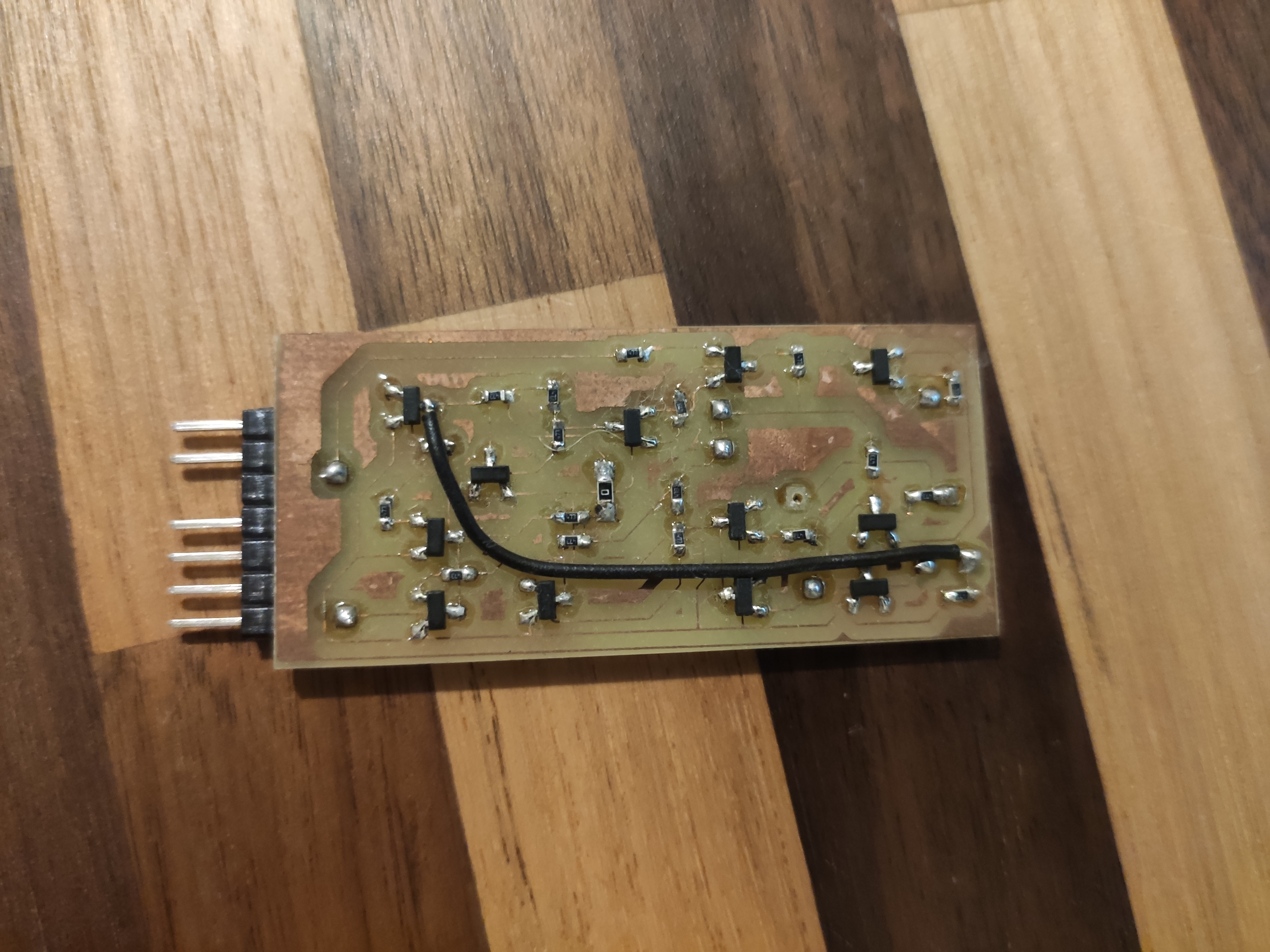
Unfortunately, the PCB and schematics are lost. So I am working on a new design:


I forgot the board in the acid.
So I got very thin lines and needed to solder an external wire.