2 byte SRAM
August 29, 2017
This project is an upgrade from the 16 bit SRAM module.
The requirements were:
- Easy stackable
- If possible, less SMD components
- Small as possible
- If a bug occurs, it must be easy to find and desolder
- No need of some extra drivers (Only a level decoder is necessary)
- As little current consumption as possible
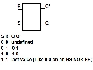
General information of a NAND FF is shown here:
RS NAND Flipflop is very common and is used in this project. A RS NOR Flipflop works too, but the hole chip would need about 2 more mosfets.
As seen in the picture above, a flipflop can switch between two states. This can be used as a memory block.
And now to the explanation, of how this thing works:
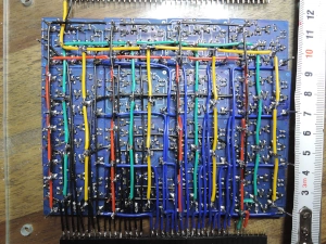
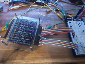
In the picture, you can see some black wires starting from the left corner. These are the inputs.
Next to them, the BLUE wires, are the output pins.
The last two, a GREEN and a RED one, are the power. (GREEN = GND, RED = Vcc)
On the top of the picture, there are the enable pins for this memory layer. The YELLOW one is the read, the black one is the write.
The design of each cell is a bit more complex. Consequently, the control is less difficult.
Everything does, what you would expect from it:
First of all, you connect the board to a power supply. (About 1.5V to 5V)
Then you mount 16 pull down resistors (60k) to the Input pins. (Because you only need them ones, it would be a waste, putting them directly on the cells)
A voltage on a input pin, is equal to 1 and vice versa.
If you want to display the output with some LEDs, you will need a transistor amplifier stage.
The last thing, is to enable / disable the read or write.
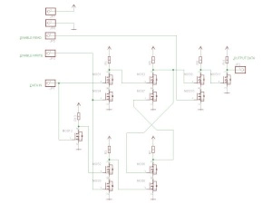
The schematic of one cell:
I tested many variations of logic gates and choosed the NAND gates. (As all the CPUs are built up with)
In the middle, there is a NAND RS flipflop. The "output enable AND gate" (NAND and a NOT gate) is on the right.
The NOT gate on the left side, switches the two inputs ON or OFF. In between you can see the access gates, connected to the "write enable" pin.
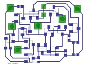
Layout:
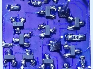
The finished circuit board uses 0603 resistors and SOT23 n-mosfets.
The "big" green squares are the access points, the two smaller ones, are used for a 0 bridge.
(The red line is a 2nd layer) I could go through a mosfet two times, but i want to be safe.
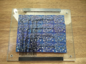
The board in real life:
The two data buses and the pull down resistors are good to locate:
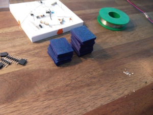
The process of creation:

